
Among the various techniques used for edge isolation in solar cell manufacturing, wet chemical edge etching remains one of the most widely adopted methods. It offers a proven balance of throughput, cost-effectiveness, and process uniformity. This article explains what edge etching is, how it isolates the front and rear junctions, which parameters affect the result, and what can go wrong when the process is not properly controlled.
Edge etching is a wet chemical process that removes unwanted doped silicon or dielectric material from the perimeter of a solar cell wafer. The goal is to eliminate any conductive bridge that may have formed between the front and rear surfaces during diffusion or thin-film deposition steps. By selectively etching the wafer edge, manufacturers create a clean electrical boundary that prevents shunting and preserves junction integrity.
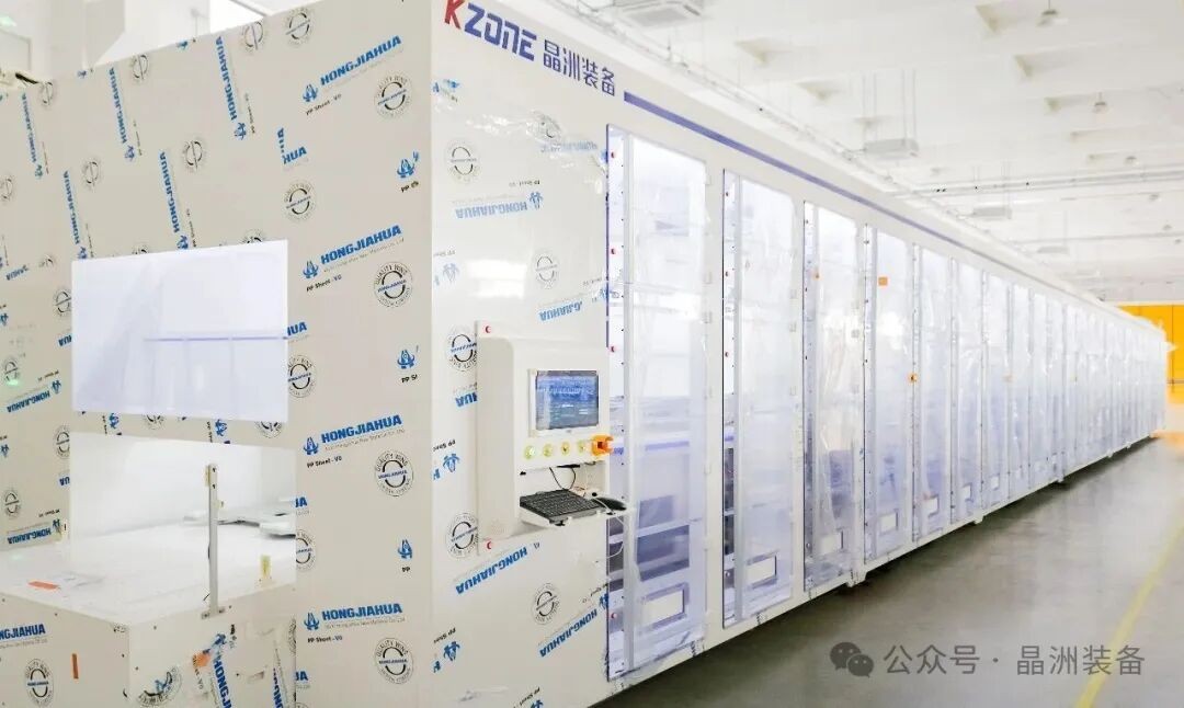
The process typically takes place in a wet bench equipped with heated chemical baths, rinse stations, and drying modules. Wafers are loaded into carriers and immersed in the etchant for a controlled period. The acid or alkaline solution attacks the exposed edge material while leaving the main front and rear surfaces largely unaffected, provided the process is optimized. In some configurations, wafers are processed with the front and rear surfaces protected by masks or by controlling the etch chemistry to preferentially remove the heavily doped edge region.
Wet chemical edge etching is especially important for high-efficiency cell concepts such as PERC, TOPCon, and IBC, where junction quality and surface passivation directly determine device performance. Even small amounts of edge shunting can lead to measurable losses in voltage and fill factor.
During boron or phosphorus diffusion, dopants can diffuse not only into the intended surface but also around the wafer edge and onto the opposite side. This creates a continuous doped path between the front emitter and the rear base or rear emitter. If left untreated, this path acts as a low-resistance channel for current leakage.
Wet chemical edge etching breaks this path by dissolving the doped silicon layer along the edge. The etchant is selected based on the type of layer being removed. Acidic mixtures such as HF/HNO3 are commonly used for silicon etching because they provide fast, isotropic removal. Alkaline solutions such as KOH or NaOH can also be used when anisotropic etching or different selectivity is required. The choice of chemistry depends on the cell architecture, the materials present on the wafer, and compatibility with upstream and downstream processes.
Because the front and rear junctions are typically located very close to the wafer edge, precision is critical. Too little etching leaves residual shunting paths, while too much etching can undercut active areas and reduce the usable surface area of the cell. Modern edge etching systems use automated transport, precise timing, and real-time bath monitoring to maintain the narrow process window required for consistent results.
Several parameters must be tightly controlled to achieve high-quality edge etching. The first is etchant concentration. As wafers are processed, the etchant becomes depleted, and reaction byproducts accumulate. Without replenishment, etch rates drift, and isolation quality becomes inconsistent. Maintaining stable concentration through automatic dosing or bath replacement is essential.
Temperature also plays a major role. Higher temperatures increase etch rates but can also increase surface roughness and chemical consumption. Most wet bench systems use heated baths with precise temperature control to keep the process within specification.
Immersion time determines how much material is removed. This parameter must be matched to the wafer thickness, doping profile, and the amount of edge wraparound. Time that is too short results in incomplete isolation, while excessive time can damage passivation layers or reduce edge strength.
Other important factors include wafer spacing, agitation level, rinse water quality, and drying method. Poor agitation can create stagnant zones where etching is non-uniform. Residual chemicals left after rinsing can cause staining or corrosion. Incomplete drying can lead to watermarks that interfere with subsequent processing steps.
When edge etching is not performed correctly, several failure modes can appear. The most common is incomplete junction isolation, where residual doped material remains along the wafer edge. This leads to increased reverse leakage current and reduced shunt resistance, both of which lower cell efficiency.
Another failure mode is non-uniform etching around the wafer perimeter. This can result from poor bath agitation, inconsistent wafer loading, or localized temperature gradients. Non-uniform edges may pass initial electrical tests but fail later under thermal cycling or field operating conditions.
Over-etching is also a concern. Excessive material removal can weaken the wafer edge and increase the risk of chipping or breakage during subsequent handling. It can also reduce the effective cell area and lower short-circuit current. In extreme cases, aggressive etching can attack active junction regions near the edge and degrade overall device performance.
Finally, contamination from the etch bath can deposit metal ions or organic residues onto the wafer surface. These contaminants can act as recombination centers, reducing minority carrier lifetime and open-circuit voltage. High-purity chemicals, filtered rinse water, and clean bath maintenance procedures are necessary to avoid this problem.
Wet chemical edge etching is a foundational process for achieving reliable junction isolation in solar cell manufacturing. By carefully controlling etchant chemistry, temperature, time, and handling conditions, manufacturers can remove unwanted edge wraparound without damaging the active cell area. For producers of PERC, TOPCon, and other advanced solar cells, investing in a well-controlled edge etching process is essential for maximizing efficiency, yield, and long-term reliability.
What chemicals are used in wet chemical edge etching?
Common chemistries include HF/HNO3 acidic mixtures for silicon etching and KOH or NaOH alkaline solutions for anisotropic etching applications.
How is etching uniformity maintained across batches?
Uniformity is maintained through temperature control, chemical replenishment, consistent immersion time, proper wafer spacing, and bath agitation.
What happens if edge etching is incomplete?
Incomplete edge etching leaves conductive paths between the front and rear junctions, causing shunting, lower shunt resistance, and reduced solar cell efficiency.