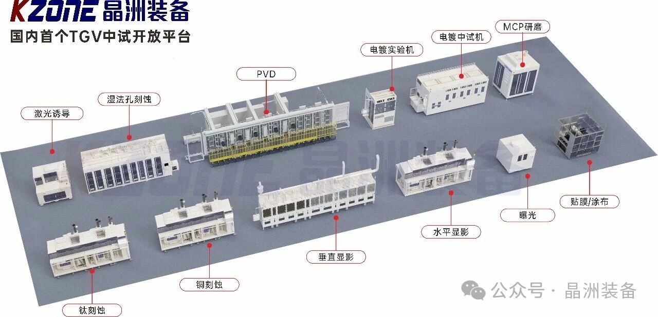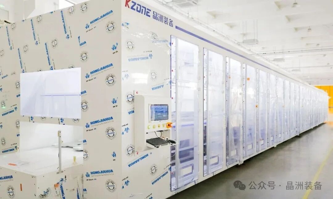

Wet processing is the umbrella term for any manufacturing step that uses a liquid chemical bath, spray, or film to clean, etch, texture, polish, or coat a substrate. It sits opposite "dry" processes such as plasma etching or physical vapor deposition, which take place in vacuum chambers using gases or ion bombardment instead of liquid chemistry. Wet processing equipment — cleaners, etchers, coaters, developers, strippers — forms the backbone of production lines across flat-panel display (FPD), photovoltaic (PV), and semiconductor manufacturing, even though the specific chemistries and substrate handling differ substantially among them.
Most wet process lines are built from a handful of recurring step types, combined and re-ordered to fit the specific product:
1. Cleaning — removing particles, organic residue, or metallic contamination between process steps, often using standard-clean chemistries like the SC-1/SC-2 (RCA) sequence.
2. Etching — selectively removing a layer of material, whether that's a doped glass byproduct like BSG on a PV wafer, a metal or ITO layer on an FPD glass substrate, or an oxide layer in semiconductor fabrication.
3. Texturing — using anisotropic or isotropic etch chemistry to create a controlled surface structure, most commonly alkaline texturing for light-trapping on PV wafers.
4. Polishing — smoothing a surface to improve subsequent layer quality, as with alkaline polishing ahead of passivation deposition.
5. Coating — applying a uniform liquid film, such as photoresist in FPD/semiconductor lithography or a slit-coated functional layer in emerging cell architectures.
The same five step types recur across all three industries, but the equipment specification changes with substrate size, geometry, and tolerance for defects. FPD wet processing handles large, thin glass substrates — from small mobile panel sizes up through G10.5 generation mother glass — where warping and breakage risk shape equipment design. Semiconductor wet processing works at a much finer feature scale with tighter particle and contamination control. PV wet processing, the focus of Kzone's TOPCon/PERC wet process solution, centers on high-volume wafer throughput: texturing, single-side etching, BSG/PSG removal, and polishing all have to run in sequence at production line speed.
Because wet process stations run in sequence, a single underperforming tool becomes the bottleneck for the entire line, and inconsistent chemistry control at any one stage can introduce defects that aren't caught until several steps later. This is why wet processing equipment is typically evaluated as an integrated line rather than a collection of standalone tools — throughput, uniformity, and chemical control at each station must all be matched to the same target line speed.
Kzone's integrated 1GW TOPCon wet process line illustrates this: chain-type single-sided etching running at 5.0+ meters per minute is paired with six-cassette alkaline polishing and RCA cleaning downstream, engineered together for a total line capacity above 18,000 182mm wafers per hour — each stage sized to match the others rather than specified in isolation. Explore Kzone's PV Industry Solutions to see how the individual wet process stages connect into a complete line.
Wet processing covers a small set of core steps — cleaning, etching, texturing, polishing, coating — applied differently across FPD, PV, and semiconductor manufacturing. Understanding how these steps connect makes it easier to evaluate any single piece of equipment in the context of the whole line. To go deeper on a specific stage, see the BSG Removal, Alkaline Polishing, or PSG Removal equipment pages, or contact Kzone's engineering team to discuss a complete line for your production target.