
As advanced packaging pushes beyond the limits of organic substrates and silicon interposers, glass has emerged as the most promising core material for next-generation chip carriers. The key enabling technology is the through glass via (TGV): a vertical via formed through the glass panel and metallized to carry signals between its two faces.
Unlike TSV (through silicon via), which relies on mature but costly deep reactive ion etching, TGV formation depends on a different toolbox — most notably laser-induced deep etching (LIDE) and a chain of wet processes that define, clean, and metallize the vias. This guide explains how TGV works, how LIDE forms vias in glass, what the wet process chain looks like, and how TGV compares with TSV on cost and performance.
A through glass via is a vertical electrical interconnect formed through a glass substrate, typically 100 µm to 700 µm thick. After the via is formed, its sidewalls are metallized — usually with copper — so signals can pass from the top surface to the bottom surface of the glass core, exactly the role a via plays in a printed circuit board or a silicon interposer.
Glass is attracting attention as a core substrate material for several structural reasons:
Electrical performance. Glass is an excellent insulator with a low dielectric constant and low loss tangent. At high frequencies, glass interconnects show significantly lower insertion loss than organic laminates and eliminate substrate‑induced losses inherent to silicon — a decisive advantage for RF, millimeter-wave, and high-bandwidth applications.
Adjustable CTE. The coefficient of thermal expansion of specialty glass can be formulated to closely match silicon (around 3 ppm/°C). This dramatically reduces warpage and thermomechanical stress when large dies or many chiplets are attached to the substrate.
Dimensional stability and flatness. Glass panels can be manufactured with outstanding flatness and surface smoothness, which is essential for fine-line redistribution layers (RDL) with line/space dimensions below 2 µm.
Panel scalability. Unlike silicon wafers, which are capped at 300 mm diameter, glass is available in large panel formats — 510 × 515 mm, 600 × 600 mm and beyond. More packages per panel translates directly into lower cost per unit.
These advantages explain why major foundries, OSATs, and substrate makers have all announced glass core substrate programs for the second half of this decade. The bottleneck has never been the material — it has been forming and metallizing high-quality vias at production cost and yield. That is where LIDE and wet processing come in.
Glass is hard, brittle, and chemically resistant. Mechanical drilling produces cracks and chipping; pure laser ablation creates heat-affected zones, recast layer, and tapered, rough holes. LIDE solves this by separating via formation into two steps: a laser modification step and a wet etching step.
In the first step, an ultrashort-pulse laser irradiates the glass along the intended via path. The laser does not remove material. Instead, it locally modifies the glass structure along a precise vertical filament, changing its chemical reactivity. A single laser pass can define thousands of via positions across a panel at very high speed, with positional accuracy measured in single-digit microns.
In the second step, the panel goes through a wet etching process, typically in a hydrofluoric acid-based chemistry. The laser-modified filaments etch at a rate orders of magnitude faster than the surrounding unmodified glass. The result is a highly selective, anisotropic etch: the vias open up along the laser-defined paths while the rest of the panel remains essentially untouched.
This two-step approach delivers via geometries that no mechanical or thermal process can match in glass:
1.Straight, vertical sidewalls with aspect ratios of 10:1 or higher — vias of 20–50 µm diameter through 300–500 µm glass.
2.Smooth sidewall surfaces with sub-micron roughness, which is critical because sidewall defects become stress concentrators and metallization weak points.
3.No microcracks, no heat-affected zone, and no recast debris, because material removal is purely chemical.
4.Tight pitch — vias can be placed close together for high I/O density, and arbitrary via layouts cost nothing extra since the laser pattern is fully programmable.
From a production standpoint, the key insight is that LIDE converts via formation into a wet etching problem. The laser step is fast and contactless; The actual material removal happens in a wet etcher, which is where throughput, uniformity, and cost per panel are won or lost.
A TGV substrate passes through a sequence of wet processes, and each one must be engineered for glass and for open vias — a very different challenge from flat-wafer processing.
Via etching. The laser-patterned panel is immersed in or sprayed with HF-based etchant. Uniformity across a large panel is the central challenge: etch rate depends on temperature, chemistry concentration, and fluid exchange at the via openings. As vias open through, the chemistry must flow through the holes to keep etching uniform from top to bottom. Production systems address this with controlled bath agitation, spray architectures that force fresh chemistry through each via, and tight temperature control, because a few tenths of a degree of variation shows up as via diameter spread across the panel.
Cleaning and surface preparation. After etching, the panel must be freed of etchant residues and particles, both on the surface and inside every via. Multi-stage cascade rinsing with resistivity monitoring, megasonic assistance to flush particles out of high-aspect-ratio holes, and reliable drying without watermarks are standard requirements. A droplet dried inside a via leaves a residue ring that can void the metallization later.
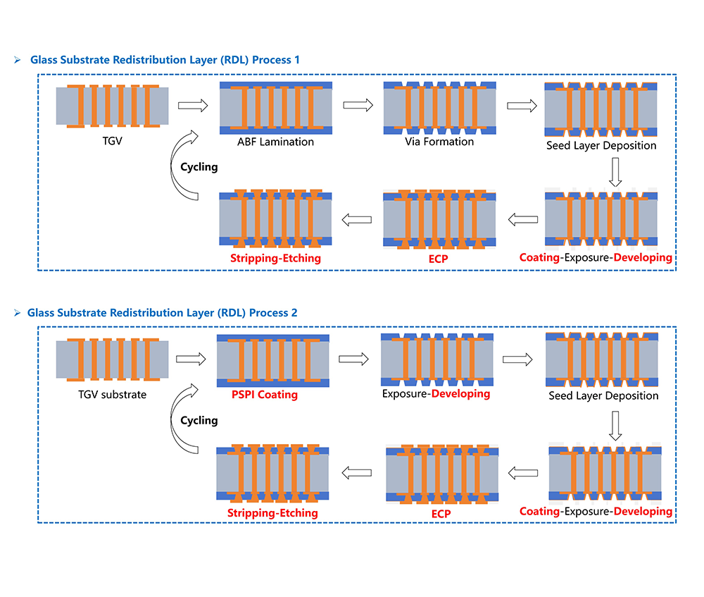
Seeding and metallization. The opened vias and panel surfaces receive an adhesion/barrier layer and a conductive seed — commonly by PVD or by electroless copper deposition — followed by electrochemical copper plating to fill or conformally coat the vias. Wet chemistry dominates this stage as well: electroless baths must wet and exchange inside every via, and plating uniformity on a large glass panel with thousands of open holes is a demanding fluid-dynamic and electrochemical problem.
Supporting wet steps. Around these core steps sit cleaning, developing, stripping, and surface treatment operations — the same family of processes used in PCB, display, and wafer-level packaging manufacturing, adapted to glass handling and via-containing substrates.
The practical conclusion for anyone planning a TGV line: via quality is made in the wet processes. The laser defines where the vias are; the etching, cleaning, and metallization equipment defines how uniform, reliable, and cost-effective they are.
How does the glass route stack up against the established silicon interposer route?
Electrical performance: Glass wins clearly for RF and high-frequency digital. Its insulating nature eliminates substrate coupling and eddy-current losses that designers must fight in silicon. TSVs in conductive silicon also need oxide liners that add capacitance and process steps.
Thermal performance: Silicon wins. Silicon conducts heat roughly 100 times better than glass, so hot dies on a glass substrate need deliberate thermal design — thermal vias, backside cooling, or copper-filled TGV arrays doubling as heat conduits.
Mechanical behavior: Glass with silicon-matched CTE minimizes warpage and stress for large packages; silicon interposers are naturally matched but limited in size. Glass panels handle like display glass: brittle but manageable with the right chucking and conveyor technology, and far larger formats are possible.
Process maturity: TSV benefits from two decades of high-volume manufacturing. TGV is newer, but LIDE-based TGV formation is arguably simpler than DRIE-based TSV: no deep silicon etch, no insulation liner deposition on sidewalls, no wafer thinning of an expensive silicon carrier.
Cost: This is the decisive factor. Silicon interposers consume prime wafers and expensive fab processes, and the 300 mm wafer format caps package size and panel efficiency. Glass material is inexpensive, LIDE plus wet etching is a comparatively low-cost patterning route, and panel processing spreads cost over far more units. For large-body, high-I/O packages, TGV on glass panels is widely expected to undercut silicon interposer cost by a wide margin once volumes ramp — which is precisely why the industry is investing in it now.
2.5D and 3D advanced packaging. Glass core substrates with TGVs are targeted at AI accelerators, HPC chiplets, and HBM-integrated packages — large interposers with fine-pitch interconnect where silicon interposer cost and reticle-size limits bite hardest. Glass panels also pair naturally with panel-level packaging flows, compounding the area-utilization advantage.
RF and millimeter-wave modules. For 5G/6G front-end modules, antenna-in-package, and radar, glass's low RF loss makes TGV substrates an ideal carrier for filters, antennas, and transceiver dies, with vias providing short, low-loss vertical transitions.
MEMS and sensors. Glass is already standard in MEMS for its optical transparency and hermeticity. TGVs add vertical electrical feedthroughs for wafer-level packaged pressure sensors, inertial sensors, microphones, and microfluidic devices, enabling true hermetic sealing with electrical I/O through the cap.
Optoelectronics and display. Optical interposers, co-packaged optics, micro-LED carriers, and image sensor packages all benefit from a substrate that is simultaneously transparent, insulating, and vertically interconnectable.
Across all of these, the common manufacturing thread is the same: LIDE-patterned vias plus a high-throughput, high-uniformity wet process chain for etching, cleaning, and metallization.
Through glass via technology turns glass from a passive carrier into an active interconnect substrate, and it is the key that unlocks glass core substrates for advanced packaging, RF, and MEMS. LIDE has emerged as the leading via formation method because it combines laser-programmable flexibility with the precision of selective wet etching — straight, smooth, crack-free vias at panel scale. But via formation is only the beginning: etching uniformity, in-via cleaning, and void-free metallization are all wet process challenges, and they determine whether a TGV line hits its cost and yield targets.