
For two decades, wafer-level packaging (WLP) has let semiconductor makers package chips while they are still on the wafer, shrinking package size and cost at the same time. But the wafer itself has become the constraint: a 300 mm disc is an awkward shape for building rectangular packages, and its area is fixed. Fan-out panel-level packaging (FOPLP) breaks that ceiling by moving the same fan-out processes from round wafers to large rectangular panels — and the cost math is compelling enough that OSATs, display makers, and substrate houses are all investing. This guide explains what panel-level packaging is, why it lowers cost per unit, how the RDL-first process flow works on panels, what equipment challenges must be solved, and who should consider the move.
Panel-Level Packaging Basics vs Wafer-Level Packaging
Fan-out wafer-level packaging (FOWLP) reconstitutes known-good dies on a round carrier, embeds them in mold compound, and then builds redistribution layers (RDL) to fan the die's I/O out to a larger pitch — all without a laminate substrate. Panel-level packaging follows the same logic but replaces the 300 mm round carrier with a rectangular panel, typically 510 × 515 mm, 600 × 600 mm, or larger.
Shape efficiency. Packages are rectangles; wafers are circles. On a round wafer, edge real estate is inherently wasted. A rectangular panel matches the package footprint, so usable area utilization jumps from roughly 85% on a wafer to well above 95% on a panel.
Process heritage. FOWLP uses wafer-fab equipment: spin coaters, steppers, wafer plating cells. FOPLP borrows its equipment DNA from the flat panel display and PCB industries, which have processed large rectangular substrates at high throughput and low cost for decades. That heritage is exactly what makes the economics work.
Importantly, panel-level packaging is not a single process but a platform: the same infrastructure serves fan-out packaging, glass core substrate fabrication, embedded die substrates, and advanced RDL interposers.
The cost argument for FOPLP rests on simple area arithmetic, but the implications run deeper.
More packages per process cycle. Moving from a 300 mm wafer to a 510 × 515 mm panel roughly triples the area; a 600 × 600 mm panel multiplies it by more than five. Since the cost of a wet process step — develop, etch, strip, plate, clean — is driven mainly by cycle time rather than substrate area, the cost per package drops almost in proportion to area gained.
Less waste at the edges. Rectangular packages on rectangular panels eliminate the partial packages and dead zones that circle-into-rectangle geometry forces on wafers. For large packages — the kind used in AI accelerators, networking, and automotive modules — the edge-loss penalty on wafers is especially severe, and the panel advantage grows with package size.
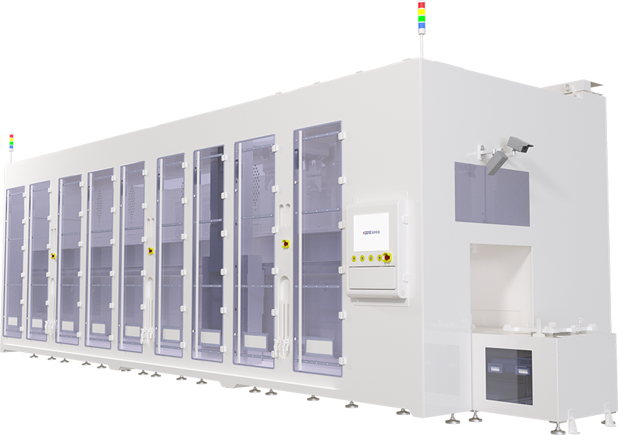
Equipment economics from the display industry. Display-grade wet process tools are built for high uptime, high throughput, and low chemical consumption per square meter. Bringing that cost structure into packaging changes the per-unit math for plating, etching, stripping, and cleaning — the wet steps that dominate RDL fabrication.
A path for large packages that wafers cannot serve. As package bodies grow beyond reticle and wafer-friendly sizes, fan-out on wafer runs out of room entirely. Panels remove the format ceiling, enabling very large multi-die packages that simply cannot be built economically at 300 mm.
Industry analyses consistently project double-digit percentage cost reductions per unit when comparable fan-out products migrate from wafer to panel — which is why the transition is being led by the most cost-sensitive, highest-volume segments first.
RDL-First Process Flow on Panels
While die-first and die-last variants exist, the RDL-first flow has become a leading architecture for panel-level fan-out because it decouples RDL yield from die attach and simplifies known-good-die economics. A typical sequence looks like this:
1.Carrier preparation. A rigid carrier panel — glass or metal — is cleaned and coated with a release layer, often by lamination or wet coating, followed by a thin adhesion/barrier stack.
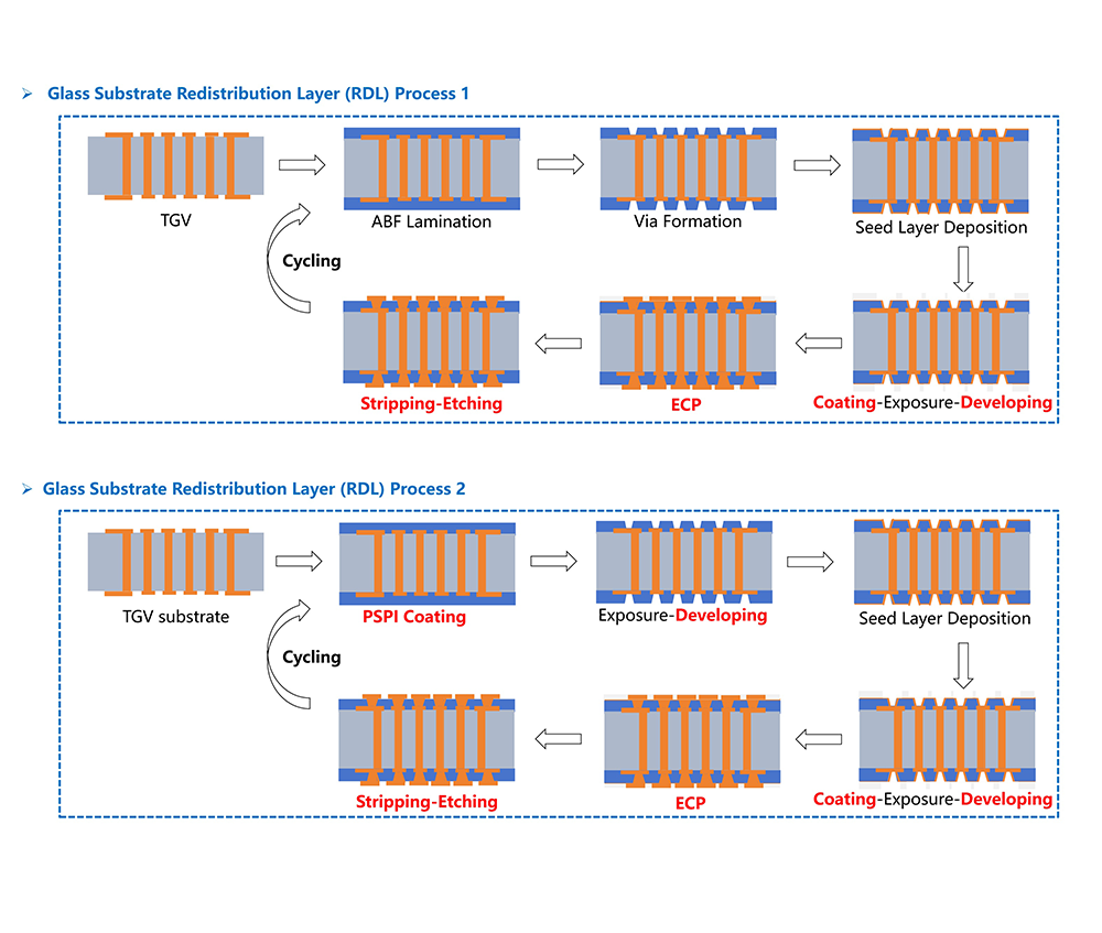
2.RDL formation. Dielectric layers and copper wiring are built directly on the carrier: dielectric coating or lamination, via patterning, seed deposition, copper electroplating, and etching or stripping to define the lines. This sequence repeats for each wiring layer, and every layer depends on wet processes — developing, cleaning, plating, etching, stripping.
3.Die attach. Known-good dies are placed face-down onto the completed RDL with flip-chip bonding. Because the RDL is already tested, die yield losses no longer destroy good wiring.
4.Molding and release. The assembly is overmolded with epoxy mold compound, then released from the carrier, leaving a molded panel with RDL on its face.
5.Backside processing and singulation. Ball attach or further passivation follows, and the panel is finally singulated into individual packages.
The unifying theme is that RDL-first on panels is fundamentally a wet process sequence. Plating uniformity, develop and etch consistency, strip completeness, and cleaning quality across the full panel area decide line/space capability and yield — exactly the disciplines that display-industry wet equipment was built to deliver.
Moving from 300 mm wafers to half-meter panels is not a simple scale-up. Three engineering problems dominate.
Warpage control. Mold compound, silicon dies, copper RDL, and a glass or organic carrier all have different thermal expansion coefficients. Across a 600 mm panel, mismatch stress translates into millimeters of bow if it is not managed — enough to break vacuum chucking, ruin lithography focus, and misalign die placement. Mitigations start with materials (low-CTE mold compounds, symmetric stack-ups) but extend deep into equipment: chucks and transport systems must hold warped panels reliably, and process tools must tolerate a substrate that is not perfectly flat.
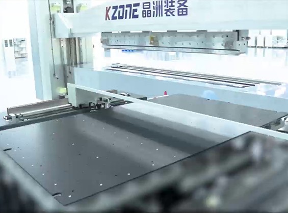
Handling thin and fragile substrates. Panels in FOPLP lines can be thin glass cores, molded reconstituted panels, or carrier-bonded assemblies — each with different fragility and edge conditions. Cassette-to-cassette automation, non-contact or edge-grip transport, and careful management of panel sag under its own weight are prerequisites for viable yield and uptime.
Large-area process uniformity. This is the heart of panel-level wet processing. On a 300 mm wafer, achieving ±3% uniformity in plating thickness or etch rate is routine; across a 600 × 600 mm panel, fluid dynamics, electric field distribution in plating, temperature gradients, and chemistry depletion all scale up as problems. Production-grade panel tools address this with engineered flow architectures, multi-zone temperature control, segmented anode designs in plating cells, and spray or immersion systems sized for full-panel coverage — technology matured in Gen 6 through Gen 10.5 display fabs and now adapted to packaging tolerances.
The equipment bar is therefore clear: panel-level lines need tools that combine display-scale uniformity and throughput with semiconductor-grade cleanliness, recipe control, and automation.
FOPLP Suitability & Adoption Timing
FOPLP is not the right answer for every package, but for several profiles the case is strong:
High-volume, cost-driven products. Power management ICs, RF front-end modules, connectivity chips, sensors, and automotive devices — segments where packaging cost is a large share of total cost and volumes justify a dedicated line.
Large-body multi-die packages. AI and HPC modules, chiplets with HBM, and networking ASICs whose package sizes strain or exceed what a 300 mm fan-out carrier can hold efficiently.
Display makers and substrate houses diversifying into packaging. Companies with existing large-panel wet process infrastructure and expertise can leverage it directly — FOPLP is the most natural adjacency for a display fab seeking semiconductor revenue.
OSATs building next-generation fan-out capacity. As wafer-level fan-out lines age and large-package demand grows, panel lines offer a capacity and cost roadmap rather than a niche experiment.
Timing matters too. FOPLP makes sense when product volumes are proven, package formats are stable, and RDL design rules are within demonstrated equipment capability. For early-stage, low-volume, or rapidly changing designs, wafer-based fan-out remains the lower-risk path.
Panel-level packaging is the industry's answer to a geometric and economic dead end: round wafers are the wrong shape and the wrong size for the next generation of high-volume, large-format packages. By moving fan-out processes to large rectangular panels, FOPLP delivers major gains in area utilization, cost per unit, and package size capability — provided that warpage, handling, and large-area uniformity are engineered under control. Those challenges are solved primarily in the wet process chain, where display-industry scale and semiconductor precision must meet.