
Chemical etching, also called wet etching, uses a liquid chemical bath or film to selectively remove material from a substrate's surface. Unlike dry or plasma etching, which relies on reactive gases or ion bombardment in a vacuum chamber, wet etching happens at atmospheric pressure through direct chemical reaction — acid or alkaline solutions dissolving specific layers while leaving others intact. It's one of the oldest and still most widely used material-removal techniques in electronics manufacturing, prized for its throughput, relatively low equipment cost, and ability to process large batches or continuous substrate flow.
The same underlying chemistry principle — selective material removal through liquid reaction — shows up across very different manufacturing contexts. In flat panel display (FPD) production, wet etchers pattern thin-film transistor circuits and remove indium tin oxide (ITO) and metal layers on glass substrates ranging from small mobile panel sizes up to G10.5 generation mother glass. In photovoltaic (PV) cell manufacturing, chemical etching removes diffusion byproduct layers like BSG and PSG and shapes wafer surface texture for light trapping. In semiconductor fabrication, wet etching cleans wafer surfaces, strips sacrificial oxide layers, and removes photoresist between lithography steps.
What changes between these applications isn't the chemistry so much as the substrate geometry and the tolerance for error. A glass panel etch for FPD deals with large, thin substrates prone to warping and breakage; a PV wafer etch has to meet single-side selectivity requirements like those used for BSG removal; a semiconductor wet etch often works at a much finer feature scale with tighter contamination control. The equipment engineering has to be tailored to each, even when the underlying reaction is conceptually similar.
Wet etching processes generally fall into two categories. Isotropic etching removes material at roughly the same rate in all directions, producing a rounded profile — this is typical of acid-based etches like the HF/HNO3 mixtures used on multicrystalline silicon or for stripping uniform layers such as BSG and PSG. Anisotropic etching removes material faster along specific crystal planes than others, producing a directional, geometrically defined profile — the classic example being alkaline (KOH/NaOH) texturing on monocrystalline silicon, which forms pyramids because it etches the (100) plane much faster than the (111) plane.
Choosing between the two isn't really a matter of preference; it's dictated by the substrate's crystal structure and the geometry the process needs. Amorphous or polycrystalline materials generally call for isotropic etching, while single-crystal materials can take advantage of anisotropic etching to create precise, repeatable structures.
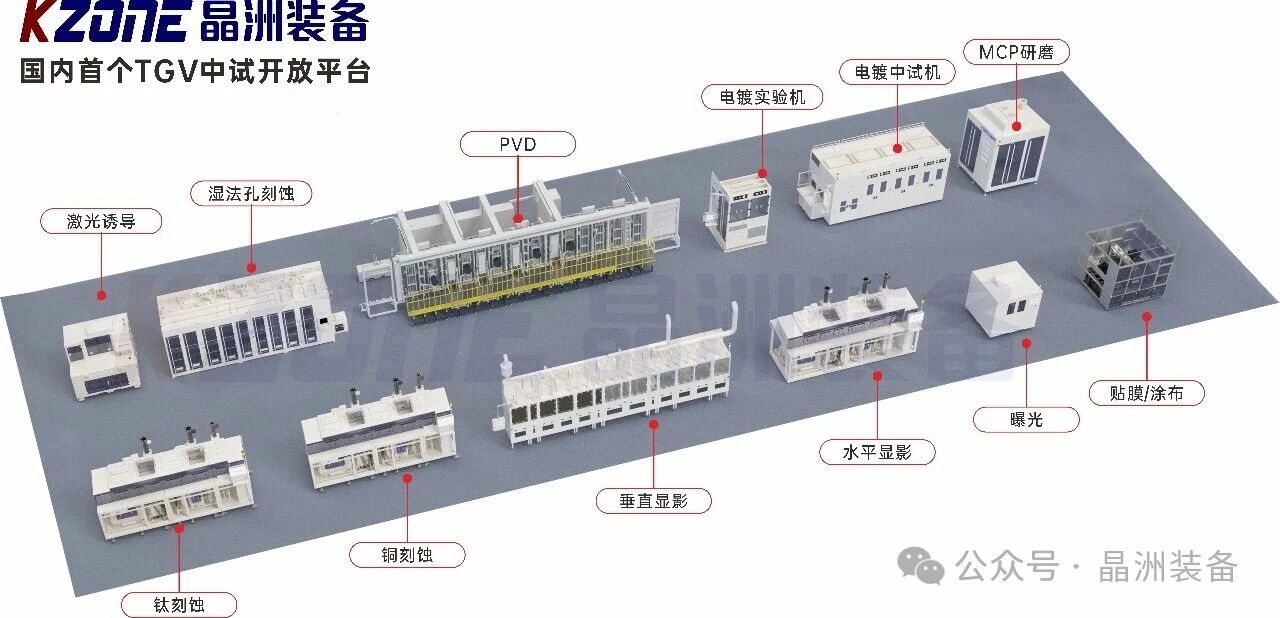
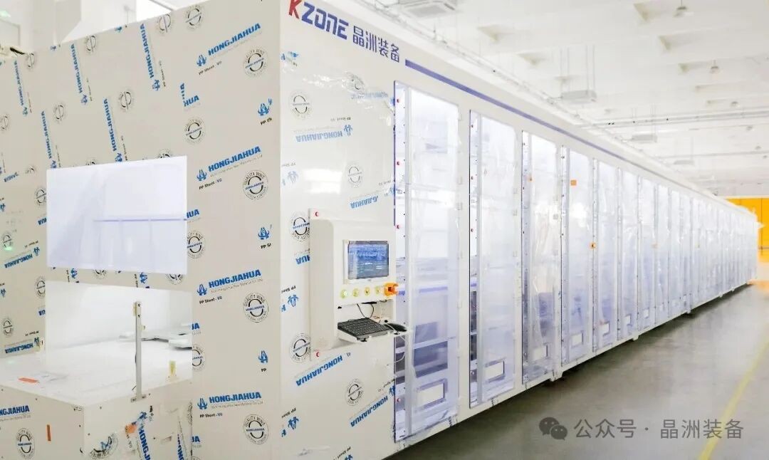
Kzone develops wet etching and cleaning equipment across all three of these industries rather than specializing in just one. In FPD, Kzone is the first and only Chinese supplier offering a full range of wet process equipment for the field's main process steps, with independently developed cleaner, coater, developer, etcher, photoresist stripper, and mask cleaner platforms spanning G2.5 through G10.5 generation glass. In PV, that same wet-process engineering underpins Kzone's TOPCon/PERC wet process solution, including texturing, BSG and PSG removal, and alkaline polishing. Kzone applies the same wet chemical process expertise to semiconductor applications as well, giving manufacturers a single technology partner across FPD, PV, and semiconductor wet processing rather than working with separate specialist vendors for each.
Chemical etching looks different from one industry to the next — glass panels, silicon wafers, semiconductor dies — but the underlying selective-removal chemistry and the equipment discipline needed to control it are closely related. To see how Kzone applies this across its PV Industry Solutions and other wet process lines, or contact Kzone's engineering team to discuss your specific etching requirements.