
As advanced packaging moves from the periphery of semiconductor manufacturing to the center of performance roadmaps — chiplets, 2.5D/3D integration, fan-out wafer and panel level packaging — electrochemical plating (ECP) has become one of its most critical unit processes. Every copper pillar, solder bump, and redistribution layer (RDL) that carries signals and power between die, interposer, and substrate is electrochemically plated. This guide explains how ECP works, its three core packaging applications, the process challenges that define plating quality, and how to choose between wafer-level and panel-level plating equipment.
Electrochemical plating deposits metal — usually copper, but also nickel, gold, tin, and solder alloys — onto a conductive seed layer by passing current through an electrolyte bath. The substrate is the cathode; metal ions in solution are reduced and build up on the seeded surface wherever current flows. Because deposition follows the electrical field and the seed layer pattern, ECP can fill features from a few micrometers to hundreds of micrometers deep with dense, high-purity, low-resistivity metal.
Advanced packaging depends on ECP for a simple reason: no alternative matches its combination of thickness capability, feature filling, film quality, and cost. PVD sputtering deposits excellent thin films but cannot economically build the 5–100+ µm copper structures that bumps, pillars, and RDL traces require. ECP delivers those structures at high deposition rates with bulk-like electrical properties, and it does so with wet process equipment that scales from 300 mm wafers to 600 × 600 mm panels.
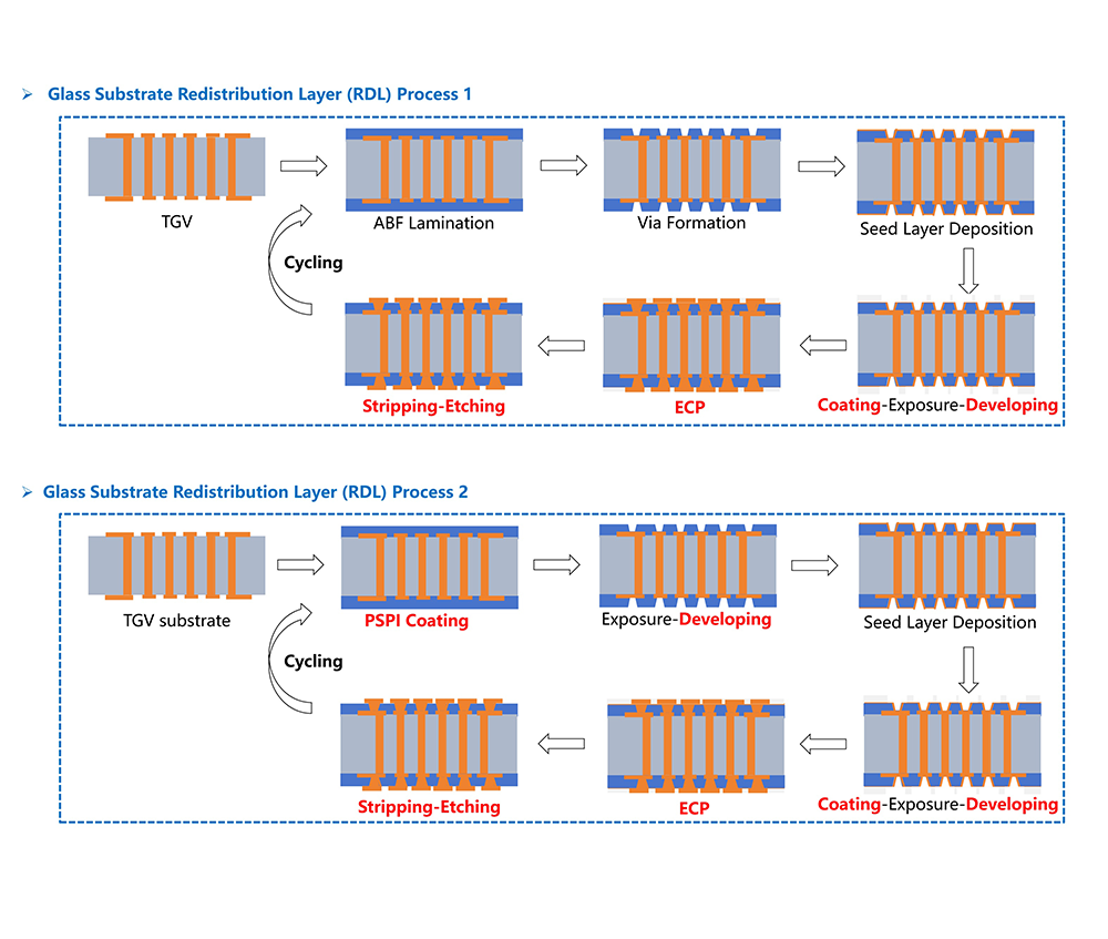
Just as important, ECP is a *patterned* process. Photoresist is applied over the seed layer, patterned by lithography, and plating fills the openings — so the quality of the plated structure is inseparable from the lithography and, later, from the photoresist stripping that removes the mold. This makes plating lines a classic wet process integration challenge: seed deposition, coating, lithography, plating, stripping, and etching must all work as one flow.
Solder bump plating is the original wafer-level packaging application. After a UBM (under-bump metallization) seed is deposited and patterned, plating builds up the bump — traditionally solder (SnAg), with a copper or nickel underlayer. Bumps of 80–150 µm pitch remain standard for flip-chip attach. The plating challenge here is alloy composition uniformity and bump height coplanarity across the wafer.
Copper pillar plating extends the bump concept for finer pitches (down to 40 µm and below). A tall, dense copper pillar — typically 20–60 µm high — is plated, then capped with a thin solder layer. Pillars give better electrical and thermal performance, finer pitch, and resistance to electromigration. They demand excellent within-feature uniformity: voids or seams inside a pillar become reliability failures under thermal cycling, and height variation translates directly into bonding yield loss.
RDL (redistribution layer) plating builds the copper wiring that reroutes die I/O to the package footprint. In fan-out packages, multiple RDL layers with line/space down to 2/2 µm and below are plated into photoresist molds over a sputtered seed. RDL plating pushes the limits in the other direction: instead of tall pillars, it must uniformly fill narrow, high-density trenches while keeping overburden minimal, because excess copper must later be removed by etch-back or CMP.
Each application places different weight on the same process levers — current density distribution, electrolyte chemistry, additive behavior, and mass transport — which is why a single plating platform must be recipe-flexible across all three.
All three applications also share the same foundation: the seed layer. A thin sputtered copper or UBM film carries the plating current and defines adhesion. Any discontinuity, oxide, or contamination on the seed shows up later as voids, skips, or peeling in the plated structure — which is why pre-plate wet cleaning and activation are treated as part of the plating process, not a separate utility step. Lines that pair plating cells with well-controlled pre-clean modules consistently show lower void rates than lines that treat them independently.
Uniformity is the headline specification. Plated thickness varies with current density, and current density varies with geometry: wafer edges plate faster than centers, isolated features plate differently from dense arrays, and large panels develop gradients from anode-to-substrate distance variation. Production control combines shielding and thief electrodes to shape the field, segmented anodes with independent current control, and optimized wafer/panel rotation and flow. State-of-the-art tools achieve within-substrate uniformity in the single-digit percent range — Kzone's ECP systems, for example, deliver plating uniformity of 7% in production, and leading wafer tools reach below 3% — a level that directly determines bump coplanarity and RDL etch-back margin.
Void control is the reliability battleground. Voids form when plating closes over a feature before filling it, usually due to additives (suppressors, accelerators, levelers) drifting out of balance, insufficient mass transport into deep features, or seed layer discontinuities. Voids in pillars cause opens or early electromigration failure; voids in RDL vias cause resistance drift. Controls include additive concentration monitoring (CVS analysis), pulse and pulse-reverse plating to improve bottom-up filling, and pre-plate seed wetting and cleaning steps.
Throwing power — the ability to deposit uniformly into recessed and high-aspect-ratio features — becomes decisive as TSVs, TGVs, and deep vias enter packaging flows. Through-glass-via (TGV) substrates, increasingly adopted for high-frequency and high-bandwidth packages, require copper filling in vias with aspect ratios of 10:1 or higher. Achieving void-free fill at these aspect ratios demands specialized chemistry, waveform control, and fixturing — capabilities Kzone has built directly into its laser-induced TGV etching and plating solutions for glass substrate packaging.
The industry's fan-out split — FOPLP (fan-out panel-level packaging) versus FOWLP (wafer-level) — is fundamentally an equipment decision.
Wafer-level plating tools run 200/300 mm wafers in single-wafer chambers with fountain or cup cell designs. They offer the finest control: precise edge exclusion, segmented anode current shaping, and the best within-wafer uniformity. For fine-line RDL below 5 µm and high-density copper pillars, wafer-level remains the reference platform.
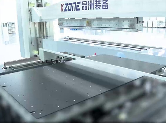
Panel-level plating tools process rectangular substrates — 310 × 310 mm, 515 × 510 mm, 600 × 600 mm — in horizontal or vertical conveyorized systems. Their value proposition is cost: one 600 × 600 mm panel holds several times the die of a 300 mm wafer, dropping per-package cost substantially at volume. The engineering challenges scale with area: maintaining current density uniformity across half a meter of substrate, handling warped reconstituted panels, and managing electrolyte flow in large cells. Modern panel platers address these with multi-zone anode control, continuous filtration and additive dosing, and automated panel handling.
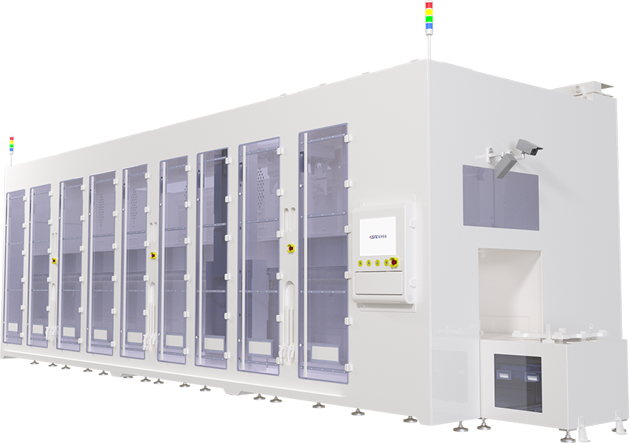
The practical choice: wafer-level for leading-edge fine-pitch and 2.5D/3D work where uniformity margin is everything; panel-level for cost-driven fan-out volume production where the format economics dominate. Many OSATs run both. Kzone supplies equipment for both camps, including FOPLP RDL plating solutions scaled for large panels — see the FOPLP RDL solution for the panel-level configuration.
When evaluating ECP equipment, structure the specification around your actual product mix:
Electrochemical plating is where advanced packaging's electrical performance is physically built — every bump, pillar, and RDL trace is a plated structure whose uniformity, void content, and fill quality were decided in the plating cell. Choosing between wafer-level and panel-level platforms is an economics-versus-resolution trade that follows your product roadmap, and specifying equipment well means demanding demonstrated performance on uniformity, chemistry control, and field shaping for your real features.
Kzone has supplied wet process equipment to more than 200 customers across semiconductor, display, and photovoltaic manufacturing since 2011, with ECP systems achieving 7% plating uniformity, TGV processing capability at 10:1 aspect ratios, and panel-level RDL plating for FOPLP production. To discuss plating equipment for your advanced packaging line — from single chambers to integrated wet process solutions — contact Kzone's engineering team.