
Photoresist stripping - (also known as photoresist removal) includes plasma ashing - is the step where the photoresist mask is taken off after it has done its job of protecting selected areas during etching, ion implantation, or plating. It sounds simple, but in high-volume semiconductor and display manufacturing, stripping is one of the most demanding wet processes in the fab: the resist must come off completely, the underlying films must not be attacked, and residues measured in nanometers can kill yield at the next step. This guide explains how the process works, how to choose between wet stripping and plasma ashing, which chemistries dominate, what defects to watch for, and what to require from stripping equipment.
Photoresist is an organic polymer film that is spin-coated, exposed, and developed to form a patterned mask. After the masked process step — plasma etching of a metal or dielectric layer, ion implantation, or wet etching — the resist has served its purpose and must be removed before the wafer or panel moves on.
In a typical flow, stripping follows every patterning step, so a single device may go through resist strip a dozen times or more. Its position in the flow matters for process design:
In flat panel display (FPD) manufacturing, the same role exists on glass substrates — TFT array and color filter processes pattern photoresist across panels from Gen 2.5 up to Gen 10.5 sizes, and every pattern step ends with a strip step. The scale differs, but the requirement is identical: complete resist removal, zero damage to ITO, aluminum, copper, or molybdenum films, and no residue.
Because stripping sits between patterning and the next deposition or implant, any residue it leaves behind is buried by the next layer — which is why stripping quality directly determines downstream yield.
There are two fundamental approaches to removing photoresist, and most fabs use both.
Plasma ashing (dry stripping) exposes the wafer to an oxygen-based plasma. Oxygen radicals oxidize the organic resist into volatile CO, CO₂, and H₂O. Downstream "ashing" systems keep the wafer outside the plasma generation zone to reduce ion bombardment damage. Ashing is fast, solvent-free, and excellent for bulk resist removal — but it cannot remove inorganic residues (metal-containing by-products, implanted dopant residues), and the plasma can oxidize or damage sensitive films such as low-k dielectrics and exposed copper.
Wet stripping uses liquid chemistries — heated solvents, amine-based mixtures, or sulfuric acid/oxidizer blends — to dissolve or lift the resist off the surface. Wet stripping excels where ashing falls short:
In practice, the most common combination is ash followed by wet clean/strip: ashing removes the bulk of the resist, and a wet step removes the remaining residues and plasma-damaged material. For many display and packaging applications, pure wet stripping in batch immersion or single-substrate spray systems remains the standard because it is gentler on metal films, easier to scale to large panel sizes, and far lower in chemical and capital cost per substrate.
Choosing a stripper chemistry means balancing three things: dissolution power against the (often hardened) resist, compatibility with every exposed film on the substrate, and rinsability — the chemistry itself must not leave a residue.
The main chemistry families in production use:
Residue control is where stripping processes are won or lost. Typical residue sources include incompletely dissolved crust flakes, redeposited resist during rinsing, and chemistry drying on the substrate between strip and rinse. Proven controls include multi-tank cascades with fresh chemistry in the final tank, continuous filtration (sub-micron) of the strip bath, controlled drain-to-rinse transfer times, and megasonic agitation to dislodge particles from features. Verification normally combines wafer surface inspection (particle counts at sub-100 nm sensitivity) with SIMS or TXRF for metallic residues when the process is critical.
The three defect classes that dominate stripping-related yield loss:
Resist residue and "veil" defects. Thin, sometimes nearly invisible organic films left in vias, trenches, or on bond pads. They show up later as high contact resistance, poor adhesion of the next deposited layer, or voids in plated features. Root causes are usually under-dosed or aged chemistry, insufficient temperature, or a crusted resist surface that the chemistry could not penetrate. Fixes: verify bath concentration and temperature control, add a plasma descum before wet strip for heavily processed resist, and confirm rinse quality.
Corrosion of exposed metal films. Aluminum and copper are attacked by the wrong chemistry, by chlorine residues from metal etch reacting with moisture, or by galvanic corrosion when dissimilar metals are exposed in the bath. Corrosion shows as pitting, haze, or resistivity drift. Fixes: select metal-compatible stripper formulations, control water content in solvent baths, minimize queue time between etch and strip, and ensure thorough DI rinse and dry.
Surface damage and film loss. Over-aggressive chemistry or excessive megasonic power can attack underlying dielectrics, roughen surfaces, or erode thin films. In FPD processes, damage to ITO or thin molybdenum layers is a classic strip-related failure. Fixes: validate etch rate of the stripper against every exposed film during process qualification, tune megasonic power, and keep strip time as short as complete removal allows.
A disciplined qualification — stripping test coupons, then measuring film thickness, sheet resistance, surface roughness, and particle counts — prevents nearly all of these defects from reaching production.
Whether the line runs silicon wafers, packaging substrates, or Gen 8.6 glass panels, production stripping equipment must deliver the same fundamentals:
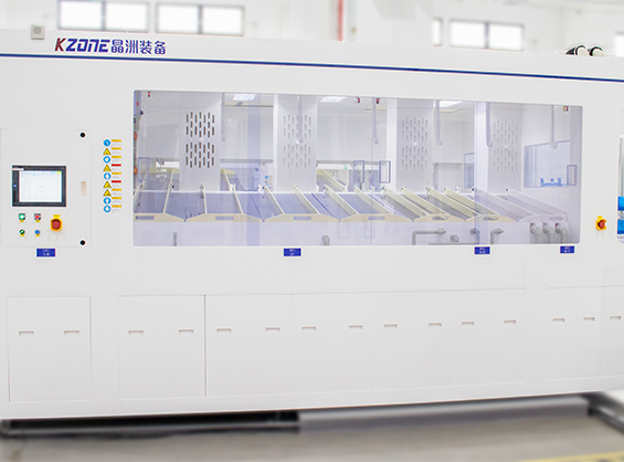
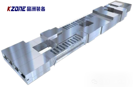
Kzone designs and manufactures a complete range of wet processing equipment for these requirements — from semiconductor photoresist strippers to large-format FPD strip and clean systems covering Gen 2.5 through Gen 10.5 panels, alongside cleaners, coaters, developers, and etchers for display, photovoltaic, and advanced packaging lines. Process modules are engineered around chemistry compatibility, bath life management, and high-throughput automation, drawing on more than a decade of wet process experience and over 400 patents. You can explore the TFT-LCD / OLED wet process solutions for a closer look at how stripping is integrated into full display production lines.
Photoresist stripping is a yield-critical step disguised as a simple one. The right approach — wet, ash, or a combination — depends on what the resist has been through and which films are exposed. Chemistry selection must balance dissolution power against film compatibility, and the real battle is fought on residue control, corrosion prevention, and surface integrity. At production scale, equipment quality decides whether the process stays in control: temperature and flow uniformity, bath management, rinse integration, and automation all translate directly into yield and cost per substrate.
If you are planning a new stripping line, upgrading an existing wet bench, or qualifying a strip process for semiconductor, display, or advanced packaging production, Kzone's engineering team can help you match chemistry, process, and equipment to your targets. Contact us to discuss your photoresist stripping requirements.