
A semiconductor wafer passes through a cleaning step before nearly every critical process stage — before oxidation, before deposition, before lithography, before implantation. Each of these steps is extremely sensitive to what's left on the wafer surface: a single sub-micron particle can print as a killer defect under a lithography mask, and trace metallic contamination can diffuse into the silicon during a later thermal step and create recombination centers that degrade device performance. Because contamination introduced at one step often isn't detected until several steps later, wafer cleaning is one of the process areas where equipment consistency has an outsized, and sometimes underappreciated, effect on overall line yield.
As feature sizes shrink and device structures become more three-dimensional, the tolerance for residual particles and contamination shrinks with them — a particle size that was harmless at an older process node can be yield-limiting at a newer one, which is part of why cleaning equipment specifications tend to tighten with each process generation rather than staying fixed.
Several distinct cleaning approaches are used across semiconductor fabs, often in combination rather than as substitutes for one another:
● RCA cleaning — the standard two-step wet chemical sequence (SC-1 for particle and organic removal, SC-2 for metallic contamination removal) that has served as the reference cleaning method since it was developed at RCA Laboratories in the late 1960s. It remains widely used as a baseline cleaning step across both semiconductor and solar wafer processing.
● Megasonic cleaning — adds high-frequency acoustic energy (typically in the 0.7–2 MHz range) to a wet chemical bath, generating microstreaming and cavitation effects that dislodge particles more effectively than chemistry alone, particularly for smaller particle sizes that basic immersion cleaning struggles to remove without risking pattern damage.
● Single-wafer cleaning: — processes one wafer at a time, typically on a spin chuck, with chemistry and rinse dispensed directly onto the rotating wafer surface. This allows tighter control over chemical exposure time and uniformity per wafer, at the cost of lower throughput per tool compared with batch immersion systems.
Batch cleaning equipment immerses a full cassette of wafers together in a shared chemical bath, offering high throughput per unit of floor space and lower chemical consumption per wafer, since many wafers share the same bath volume. The trade-off is less precise control over any individual wafer's exposure — all wafers in the cassette experience essentially the same process conditions, which can be a limitation for processes requiring wafer-to-wafer or even within-wafer precision.
Single-wafer cleaning equipment processes wafers individually, which allows chemistry, rinse, and dry conditions to be tuned wafer by wafer if needed, and generally supports tighter uniformity control across the wafer surface. It trades away some of batch processing's throughput and chemical efficiency in exchange for that precision, which is why single-wafer tools tend to be specified for the most critical, defect-sensitive cleaning steps, while batch tools continue to handle higher-volume, less critical cleaning stages.
Two categories of performance metrics dominate how cleaning equipment is evaluated:
● Particle removal efficiency (PRE) — typically measured as the percentage of particles above a given size threshold removed per cleaning cycle, benchmarked against pre- and post-clean wafer particle counts. As critical particle size thresholds shrink with each process node, PRE requirements at smaller size bins become correspondingly more demanding.
● Metallic contamination control — measured via trace metal analysis (such as ICP-MS) of the wafer surface after cleaning, tracking specific elements (iron, copper, nickel, and others) known to create deep-level defects in silicon. Consistent metallic contamination control depends as much on equipment material selection and chemical delivery system cleanliness as on the cleaning chemistry itself, since a cleaning tool can reintroduce contamination from its own wetted components if they aren't specified correctly.
Both metrics are only meaningful when measured consistently over time — a tool that performs well on a qualification run but drifts under continuous production use hasn't actually solved the contamination control problem, which is why repeatability across long production runs matters as much as peak performance on a single test wafer.
A few practical questions help narrow down the right cleaning equipment architecture for a given process step:
● Does this step's defect sensitivity justify single-wafer precision, or can batch throughput handle it without compromising yield?
● What particle size and metallic contamination thresholds does this process node require, and does the equipment's demonstrated PRE and trace-metal performance meet them with margin, not just on paper?
● How will the equipment's wetted materials and chemical delivery system be qualified for contamination control, and what's the track record for maintaining that control over extended production runs?
● How does this cleaning stage's throughput align with the rest of the line, so it doesn't become a bottleneck as volume scales?
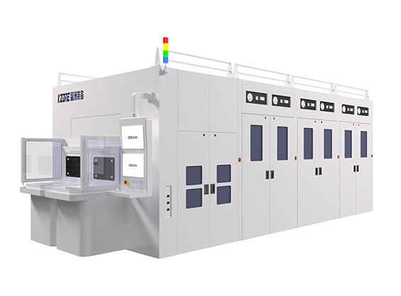
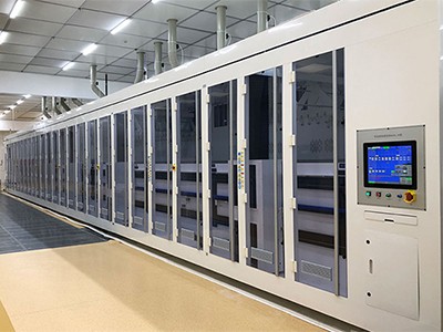
Kzone applies its wet process equipment engineering — developed across FPD, PV, and semiconductor applications — to cleaning systems designed around these considerations. See Kzone's Semiconductor Solutions for the current equipment lineup.
Wafer cleaning sits quietly behind nearly every critical step in semiconductor manufacturing, and the choice between RCA, megasonic, batch, and single-wafer approaches has a direct, if sometimes delayed, effect on yield. Matching the cleaning architecture to each process step's defect sensitivity — rather than defaulting to one approach across the whole line — is usually the more reliable path to consistent results. To review equipment options or discuss requirements for a specific process node, explore Kzone's Semiconductor Solutions, or contact Kzone's engineering team for a cleaning equipment consultation.